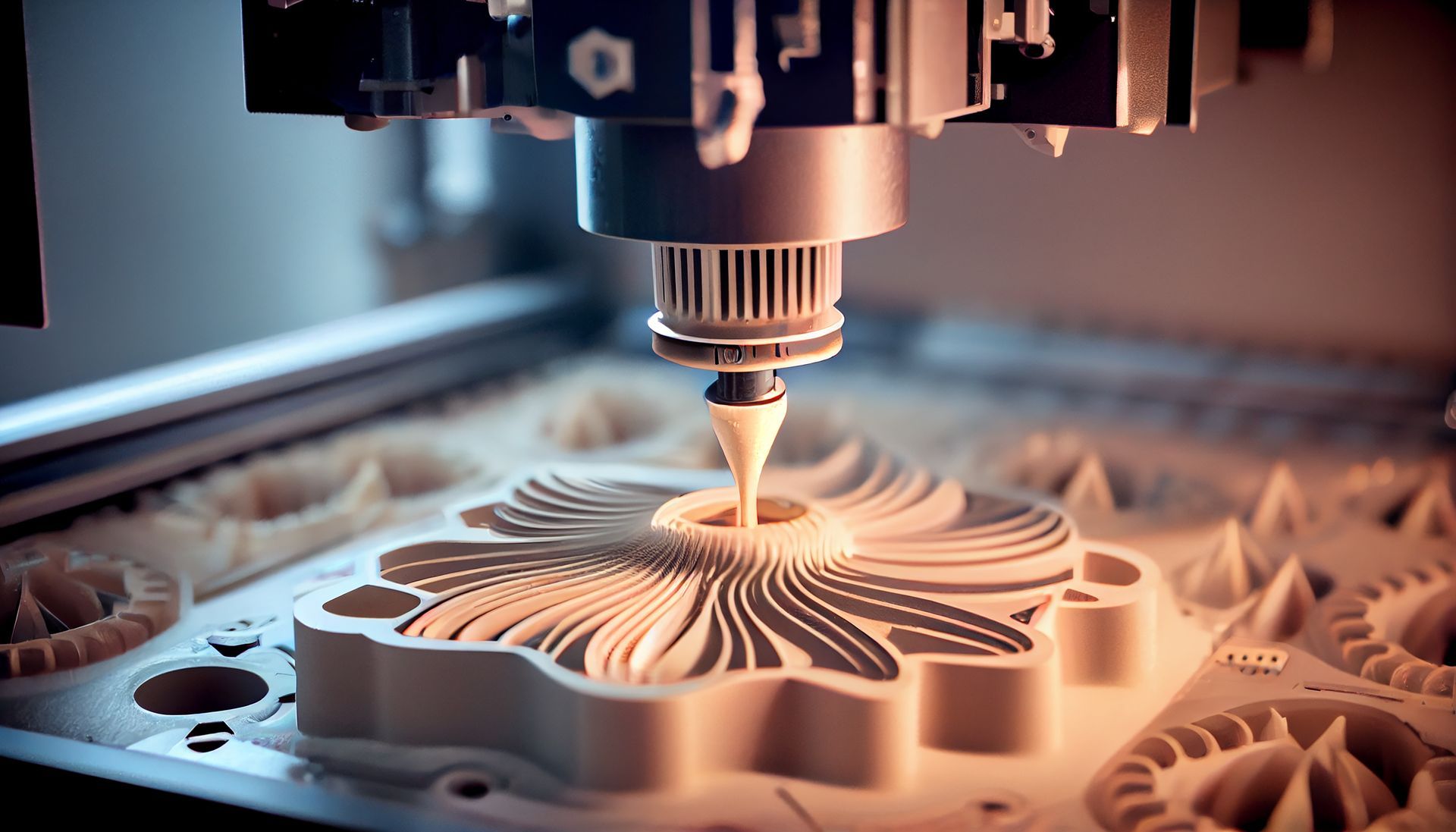
Nanofabrication is a groundbreaking discipline that holds immense potential for revolutionizing various industries. It involves the manufacture of structures and devices on the nanoscale, often employing sophisticated techniques to manipulate materials at the atomic and molecular levels. The term “nano” refers to one billionth of a meter, signifying the minuscule dimensions in which nanofabrication operates. This cutting-edge field has opened up a world of possibilities, enabling the creation of novel materials, advanced electronics, biomedical devices, and much more.
Nanofabrication has come a long way since its inception, with significant advancements over the years that have unlocked a plethora of opportunities. The process typically involves top-down or bottom-up approaches, or a combination of both, to engineer nanostructures with precision and control. In the top-down approach, larger materials are downsized through techniques like etching or lithography, while the bottom-up approach builds structures from atomic or molecular components, such as self-assembly or chemical vapor deposition.

What is Nanofabrication?
Nanofabrication is a process of manufacturing structures, devices, and materials on the nanoscale, typically ranging from 1 to 100 nanometers. It involves the precise manipulation and control of materials at the atomic or molecular level to create complex and functional nanostructures. Nanofabrication plays a crucial role in various fields, including electronics, photonics, medicine, energy, and materials science.
There are two primary approaches to nanofabrication: the top-down approach and the bottom-up approach. The top-down approach involves starting with a larger structure or material and then reducing it in size to create nanostructures. This approach is similar to conventional microelectronic processing technologies, where larger machines are used to build smaller ones, enabling the creation of intricate nanoelectronic components and devices. Techniques such as photolithography and etching are commonly used in top-down nanofabrication. However, the top-down approach has limitations in terms of resolution and scalability, particularly when dealing with nanoscale features.
On the other hand, the bottom-up approach involves assembling nanostructures from individual atoms or molecules. It takes advantage of chemical or physical interactions to organize and arrange the components in a predetermined manner, creating complex structures with exceptional precision. This approach allows for the formation of nanostructures with covalent bonds, which are far stronger than forces experienced in macroscale components. Bottom-up nanofabrication techniques include chemical vapor deposition (CVD), physical vapor deposition (PVD), self-assembly, and epitaxial growth.
What nanomachines promise for the humanity
A combination of both top-down and bottom-up approaches is often employed to fabricate intricate and functional nanostructures. The ability to integrate these approaches provides greater flexibility and enhances the capability of nanofabrication.
In the top-down approach, the process typically starts with a substrate, such as a silicon wafer, which serves as the base material. The substrate undergoes several steps, including deposition of thin films, patterning through techniques like photolithography, and etching to remove unnecessary material, creating the desired nanoscale features. The latest generation of optical nanolithography systems utilizes X-ray, extreme ultraviolet (EUV), or charged particle beams to achieve nanoscale patterning with high spatial resolution.
In the bottom-up approach, nanofabrication involves the controlled assembly of individual atoms or molecules to build complex nanostructures. This process requires careful design and manipulation of chemical reactions or self-assembly processes to achieve the desired structure and properties. Techniques like chemical vapor deposition (CVD) allow for the growth of thin films by supplying reactant gases that form nanostructures on the substrate surface.
Multi-tech means multi-use
Nanofabrication of functional micro/nano-features has become increasingly relevant in various fields such as electronics, photonics, energy, and life sciences. The ability to create novel nanostructures and architectures using innovative synthesis, fabrication, and manufacturing methods enables the control of material properties and opens up new applications.
Imprinting techniques
Imprinting techniques involve creating patterns on materials by using templates or molds. These methods include nanoimprint lithography (NIL), soft lithography, and microcontact printing. NIL, in particular, offers high resolution and is cost-effective for mass production, making it suitable for nanoscale patterning in the semiconductor and photonic industries. Soft lithography, on the other hand, is versatile and can produce complex nanostructures, making it valuable for biological and biomedical applications.
Electron Beam Lithography (EBL)
EBL uses a focused electron beam to create patterns on a substrate. It provides high-resolution patterning at the nanoscale and is widely used in research and development of nano-devices, as well as in the fabrication of photonic and optoelectronic devices. However, EBL is relatively slow, limiting its application for large-scale production.

Chemical Vapor Deposition (CVD)
CVD is a bottom-up nanofabrication technique that involves the deposition of thin films of materials on a substrate. It can be used to grow various nanomaterials, such as graphene and carbon nanotubes, with precise control over their size and structure. CVD finds applications in electronics, energy storage, and catalysis.
Self-assembly techniques
Self-assembly methods rely on the spontaneous arrangement of nanoscale building blocks into desired patterns. This approach is particularly useful for creating periodic structures and nanostructured materials. Block copolymer lithography is a self-assembly technique that has shown promise in nanofabrication for applications in nanoelectronics and data storage devices.
Photolithography
Photolithography is a top-down technique used in the semiconductor industry for large-scale fabrication. It involves using masks and light to pattern a photosensitive material on a substrate. While traditional photolithography has limitations in achieving nanoscale features, advanced techniques like extreme ultraviolet lithography (EUV) have enabled nanoscale patterning for high-performance integrated circuits.
Atomic Layer Deposition (ALD)
ALD is a precise nanofabrication method that allows the deposition of thin films with atomic-scale control. It is widely used in semiconductor manufacturing for gate oxide deposition and in the development of nanoscale electronic devices. ALD is also used in applications such as nanoscale coatings and energy storage materials.
These nanofabrication techniques open up exciting possibilities for developing advanced materials and devices with unprecedented properties. From electronics and photonics to energy and life sciences, nanofabrication plays a crucial role in shaping the future of technology and innovation.
As researchers come up with new nanoscale engineering ideas, the potential for groundbreaking applications across various industries becomes increasingly promising.

Nanofabrication in electronics and beyond
The electronics industry has been one of the primary beneficiaries of nanofabrication. As semiconductor devices have shrunk to nanometer scales, Moore’s Law has continued its remarkable trajectory, fostering exponential growth in computing power. The integration of nanoscale transistors on microchips has led to faster, more energy-efficient devices that have shaped our digital age.
Furthermore, nanofabrication has enabled the creation of nanoelectromechanical systems (NEMS) and nanophotonic devices, providing opportunities for new functionalities. For instance, NEMS offer ultra-sensitive sensors and actuators, with potential applications in healthcare, environmental monitoring, and communication systems.
The unique properties of nanomaterials have intrigued scientists and engineers alike. By manipulating materials at the nanoscale, novel characteristics emerge, altering their behavior and interactions. For example, carbon nanotubes have exceptional mechanical strength and electrical conductivity, making them ideal candidates for reinforced composites and high-performance electronic components.
The use of nanomaterials has extended to various sectors, such as medicine, energy, and environmental remediation. In the medical field, nanoparticles have opened new avenues for targeted drug delivery, imaging agents, and disease diagnosis. In energy, nanofabrication has facilitated advancements in solar cells, batteries, and fuel cells, paving the way for sustainable energy solutions.

Too good to be true
Despite significant progress in nanofabrication technologies, there remain hurdles and limitations that researchers and engineers are working to overcome. Here are some of the challenges in nanofabrication.
Resolution and feature size control
Achieving high resolution and precise control over feature sizes at the nanoscale is a fundamental challenge. Techniques like electron beam lithography (EBL) and focused ion beam (FIB) lithography have been successful in creating nanostructures, but they are often serial processes with low throughput. Developing parallel nanofabrication methods that can achieve high resolution and feature size control over large areas is an ongoing challenge.
Throughput and Cost: Many nanofabrication techniques, such as EBL and FIB, have limited throughput and can be expensive to implement. For widespread adoption and large-scale production of nanodevices, it is essential to develop cost-effective and high-throughput nanofabrication methods.
Materials compatibility
Some nanofabrication techniques may be limited in their ability to work with certain materials. Ensuring compatibility with a wide range of materials is crucial for diverse applications in electronics, photonics, and biomedical fields.
Scalability
While laboratory-scale nanofabrication methods have shown promising results, scaling up to industrial-level production can be challenging. Bridging the gap between research-scale fabrication and large-scale manufacturing is essential for commercializing nanotechnology-based products.
Uniformity and reproducibility
Achieving uniformity and reproducibility of nanostructures across large areas is critical for reliable device performance and mass production. Controlling variations and defects in nanofabrication processes is an ongoing challenge.
Integration with existing technologies
Integrating nanofabricated components with existing technologies and manufacturing processes can be complex. Compatibility and seamless integration with conventional microfabrication methods are crucial for practical applications.

Metrology and characterization
Characterizing nanoscale features and measuring their properties accurately is challenging. Developing advanced metrology techniques that can efficiently characterize nanostructures is important for quality control and process optimization.
Environmental and health concerns
As nanofabrication technologies advance, there is a need to address potential environmental and health concerns associated with the production and disposal of nanomaterials. Ensuring the safe and sustainable development of nanofabrication processes is vital for responsible technology deployment.
Multiscale patterning
Integrating multiple scales of patterning, from nanometer to micrometer, is essential for creating complex functional structures and devices. Developing techniques that seamlessly combine different length scales in a single process is a significant challenge.
Manufacturability and standardization
Establishing standardized nanofabrication processes and protocols is crucial for ensuring the manufacturability and reproducibility of nanotechnology-based products. Efforts to create industry standards for nanofabrication are ongoing.
Demand for nanofabrication engineers on the rise
As of 2023, nanofabrication engineering has the potential to offer a promising career path. Nanotechnology, which is at the core of nanofabrication engineering, is an evolving and cutting-edge field that has the potential to reshape industries and bring transformative innovations to various sectors.
Nanofabrication engineers play a crucial role in creating nanodevices, nanostructures, and nanomaterials that have applications in electronics, photonics, medicine, energy, and many other fields. The field of nanofabrication is crucial for advancing technologies like nanoelectronics, nanophotonics, and nanomedicine, among others.
The job market for nanotechnology professionals may still be relatively niche, and job opportunities might not be as abundant compared to more established fields. Despite these initial challenges, the demand for nanotechnologists and nanofabrication engineers is on the rise. As industries increasingly recognize the potential of nanotechnology and its applications, there is a growing need for skilled professionals who can design, develop, and implement nanofabrication techniques and technologies.

Nanofabrication engineers can find opportunities in various sectors, including research and development, manufacturing, healthcare, and academia. The interdisciplinary nature of nanotechnology allows for collaborations with scientists, engineers, and professionals from diverse backgrounds, making the work environment dynamic and intellectually stimulating.
The salaries for nanotechnology professionals can vary based on factors such as education, experience, and location. The approximate salary ranges for nanotechnology professionals in countries like the USA, Canada, Great Britain, and Australia vary depending on career level, with entry-level positions generally offering lower salaries than mid-career and experienced positions.
Here are the approximate salary ranges for nanotechnology professionals in the USA and Canada, according to Glassdoor:
The USA:
- Entry-level: $60,000 – $80,000 per year
- Mid-career: $80,000 – $120,000 per year
- Experienced: $120,000 – $180,000 per year
Canada:
- Entry-level: CAD 50,000 – CAD 70,000 per year
- Mid-career: CAD 70,000 – CAD 100,000 per year
- Experienced: CAD 100,000 – CAD 140,000 per year
While the field of nanofabrication engineering may still be relatively new, it holds significant promise for those who are passionate about cutting-edge technologies and scientific breakthroughs.
As industries continue to invest in nanotechnology research and development, the career prospects for nanofabrication engineers are likely to improve, presenting exciting opportunities for professionals interested in this field.
Featured image credit: Freepik.


